US7321637B2 - Data slice control device and control method - Google Patents
Data slice control device and control method Download PDFInfo
- Publication number
- US7321637B2 US7321637B2 US11/041,215 US4121505A US7321637B2 US 7321637 B2 US7321637 B2 US 7321637B2 US 4121505 A US4121505 A US 4121505A US 7321637 B2 US7321637 B2 US 7321637B2
- Authority
- US
- United States
- Prior art keywords
- data
- circuit
- signal
- monotone
- period
- Prior art date
- Legal status (The legal status is an assumption and is not a legal conclusion. Google has not performed a legal analysis and makes no representation as to the accuracy of the status listed.)
- Expired - Fee Related, expires
Links
Images


Classifications
-
- H—ELECTRICITY
- H04—ELECTRIC COMMUNICATION TECHNIQUE
- H04N—PICTORIAL COMMUNICATION, e.g. TELEVISION
- H04N7/00—Television systems
- H04N7/025—Systems for the transmission of digital non-picture data, e.g. of text during the active part of a television frame
- H04N7/035—Circuits for the digital non-picture data signal, e.g. for slicing of the data signal, for regeneration of the data-clock signal, for error detection or correction of the data signal
- H04N7/0355—Circuits for the digital non-picture data signal, e.g. for slicing of the data signal, for regeneration of the data-clock signal, for error detection or correction of the data signal for discrimination of the binary level of the digital data, e.g. amplitude slicers
Definitions
- the present invention relates to a device and a method for controlling a slice level of data which are serially transmitted and, more particularly, to those for controlling a slice level of text data of telecast which are transmitted utilizing a vertical blanking period of a video signal.
- a telecast mode for transmitting data of telecast utilizing a vertical blanking period of a video signal has generally been known as a method for transmitting data using serial transmission.
- data of telecasts are transmitted utilizing vertical blanking periods of video signals.
- FIG. 15 shows the types of telecasts employed in the respective regions in the world, superimposition lines where telecasts are superimposed, and transmission clocks.
- a data slice control device as shown in FIG.
- a video signal input terminal 1401 receives an analog video signal S 1401 in which telecast data are superimposed in a vertical blanking period.
- An A/D converter 1402 samples the analog video signal S 1401 with a predetermined sampling clock fs (MHz) to convert the analog video signal S 1401 into a digital video signal S 1402 , and outputs the digital video signal S 1402 to a low-pass filter (LPF) 1403 .
- fs sampling clock
- LPF low-pass filter
- the LPF 1403 subjects the inputted digital video signal S 1402 to noise removal, and outputs the noise-removed digital video signal S 1403 to a maximum value detection circuit 1404 , a minimum value detection circuit 1405 , and a binarization circuit 1414 .
- a sync separation circuit 1419 separates the inputted digital video signal S 1402 into a horizontal sync signal S 1419 a and a vertical sync signal S 1419 b , and outputs these signals to a clock run-in (CRI) period setting circuit 1418 .
- the horizontal sync signal S 1419 a and the vertical sync signal S 1419 b are used for setting the position of a CRI period.
- the CRI period setting circuit 1418 generates a CRI period setting signal S 1418 for setting a CRI period of the telecast data superimposed on the digital video signal S 1402 , on the basis of the vertical sync signal S 1419 b and the horizontal sync signal S 1419 a , and outputs the CRI period setting signal S 1418 to the maximum value detection circuit 1404 and the minimum value detection circuit 1405 .
- the maximum value detection circuit 1404 detects a maximum value S 1404 of the amplitudes at the sampling points of the digital data within the period that is set by the CRI period setting signal, on the basis of the CRI period setting signal S 1418 obtained from the CRI period setting circuit 1418 and the noise-removed digital video signal S 1403 , and outputs the maximum value S 1404 to a slice level calculation circuit 1413 .
- the minimum value detection circuit 1405 detects a minimum value S 1405 of the amplitudes at the sampling points of the digital data within the period that is set by the CRI period setting signal, on the basis of the CRI period setting signal S 1418 obtained from the CRI period setting circuit 1418 and the noise-removed digital video signal S 1403 , and outputs the minimum value S 1405 to the slice level calculation circuit 1413 .
- the slice level calculation circuit 1413 calculates a slice level S 1413 using the maximum value S 1404 and the minimum value S 1405 , and outputs the slice level S 1413 to the binarization circuit 1414 .
- the binarization circuit 1414 converts the noise-removed digital video signal S 1403 into a binarized signal S 1414 comprising 0 and 1 at the slice level S 1413 , and outputs the binarized signal S 1414 to a sampling circuit 1415 .
- the sampling circuit 1415 samples the binarized signal S 1414 that is obtained in the binarization circuit 1414 , at predetermined sampling intervals according to the type of the telecast mode, and outputs sampled data S 1415 to a decoding circuit 1416 .
- the decoding circuit 1416 converts the serial sampled data S 1415 into a parallel signal, subjects the parallel signal to a decoding process according to the telecast type, such as error correction, and outputs the decoded data S 1416 through an output terminal 1417 to the outside.
- the CPI period setting signal is generated on the basis of the horizontal sync signal obtained from the sync separation circuit, and a maximum value and a minimum value of the amplitudes of the data within the period indicated by the CRI period setting signal are calculated, and then the slice level of the telecast data is calculated using the maximum value and the minimum value. Therefore, the following drawbacks may occur.
- the horizontal sync signal separated by the sync separation circuit may be disturbed by such as a macrovision signal of a copy guard signal that is superimposed in the vertical blanking period. Then, the CRI period setting signal is also disturbed, whereby the CRI period setting signal cannot be generated in a desired position, and an optimum slice level cannot be calculated.
- the present invention is made to solve the above-described problems and has for its object to provide data slice control device and method which are able to calculate an accurate slice level even when the horizontal sync signal and the CRI period setting signal are disturbed by a macrovision signal or the like.
- a data slice control device comprises: an A/D converter for sampling a data signal transmitted in serial, with a sampling clock of a predetermined frequency, thereby converting the data signal into digital data; a period setting circuit for setting a predetermined period of the data signal; a monotone increase detection circuit for detecting a monotone increase detection point indicating that amplitude values of sampling points of the digital data continuously increase within the period that is set by the period setting circuit; a monotone decrease detection circuit for detecting a monotone decrease detection point indicating that amplitude values of sampling points of the digital data continuously decrease within the period that is set by the period setting circuit; a counter for performing counting with the sampling clock during the period that is set by the period setting circuit, while resetting the count at a timing when the monotone increase detection circuit detects the monotone increase detection point; a data holding circuit for holding count data obtained from the counter, at a timing when the monotone decrease detection circuit detects a monotone decrease detection point; a period determination circuit for determining
- a data slice control device further comprises: a determination result counter for counting the result of determination obtained from the period determination circuit; an accumulation circuit for accumulating the slice levels obtained from the slice level calculation circuit; and a data selection circuit for selecting a slice level on the basis of the accumulated data obtained from the accumulation circuit, and the determination result count data obtained from the determination result counter. Therefore, even when the data signal is disturbed due to ghosts or noises during a predetermined period (CRI period or framing code period), slice levels can be calculated in a predetermined period including the same frequency component, and the average of the slice levels can be obtained. As a result, a more accurate slice level can be calculated while reducing adverse effects of ghosts and noises.
- the data signal transmitted in serial is a telecast signal that is superimposed in a vertical blanking period of a video signal and transferred.
- the period setting circuit sets a transmission clock synchronization period in which the transmission clock of the data signal is synchronized with the sampling clock.
- a data slice control device comprises: an A/D converter for sampling a data signal transmitted in serial, with a sampling clock of a predetermined frequency, thereby converting the data signal into digital data; a period setting circuit for setting a predetermined period of the data signal; a coring circuit for subjecting the digital data to a coring process; a first masking circuit for subjecting coring data, which is obtained from the coring circuit within the period set by the period setting circuit, to a masking process; a first delay unit for delaying the masking-processed coring data obtained from the first masking circuit, by one sampling clock; a second delay unit for delaying the delayed data obtained from the first delay unit, by another one sampling clock; an operation unit for arithmetically processing the masking-processed coring data obtained from the first masking circuit, and the delayed data obtained from the second delay unit; a shifting operation circuit for subjecting operation result data obtained from the operation unit to a shift operation process; a determination unit for detecting
- a slice level can be detected only in the slice level detection range with data outside the detection range being ignored. Further, since the inclinations of monotone increase and monotone decrease of the digital data are calculated using the determination unit and the comparator, more accurate detection of monotone increase and decrease can be carried out. Furthermore, since the digital data is subjected to coring, adverse effects of noises equal to or lower than the pedestal level can be reduced. As a result, a more accurate slice level can be calculated.
- the data slice control device further comprises: a determination result counter for counting the result of determination obtained from the period determination circuit; an accumulation circuit for accumulating the slice levels obtained from the slice level calculation circuit; and a data selection circuit for selecting a slice level on the basis of the accumulated data obtained from the accumulation circuit, and the determination result count data obtained from the determination result counter. Therefore, even when the data signal is disturbed due to ghosts or noises during a predetermined period (CRI period or framing code period), slice levels can be calculated in a predetermined period including the same frequency component, and the average of the slice levels can be obtained. As a result, adverse effects of ghosts and noises can be reduced. Furthermore, since the digital data is subjected to coring, adverse effects of noises equal to or lower than the pedestal level can be reduced. As a result, a more accurate slice level can be calculated.
- the data signal transmitted in serial is a telecast signal that is superimposed in a vertical blanking period of a video signal, and transmitted.
- the period setting circuit sets a transmission clock synchronization period in which the transmission clock of the data signal is synchronized with the sampling clock.
- a data slice control method comprises: an A/D conversion step of sampling a data signal transmitted in serial, with a sampling clock of a predetermined frequency, thereby converting the data signal into digital data; a period setting step of setting a predetermined period of the data signal; a data storage step of storing the digital data within the period that is set in the period setting step; an address generation step of generating storage addresses of the digital data that is stored in the data storage step; a maximum value detection step of detecting a maximum value of the amplitude values of the digital data stored in the data storage step; a minimum value detection step of detecting a minimum value of the amplitude values of the digital data stored in the data storage step; a monotone increase point address detection step of detecting a storage address of a monotone increase point indicating that the amplitude values of the sampling points of the digital data stored in the data storage step continuously increase; a monotone decrease point address detection step of detecting a storage address of a monotone decrease point indicating that the
- the data slice control method further comprises: a determination result counting step of counting the result of determination obtained in the determination step; an accumulation step of accumulating the slice levels obtained in the slice level calculation step; and a slice level operation step of arithmetically processing the slice levels on the basis of the accumulated data obtained in the accumulation step, and the determination result count data obtained in the determination result counting step. Therefore, even when the data signal is disturbed due to ghosts or noises during a predetermined period (CRI period or framing code period), slice levels can be calculated in a predetermined period including the same frequency component, and the average of the slice levels can be obtained. As a result, a more accurate slice level can be calculated while reducing adverse effects of ghosts and noises.
- the data signal transmitted in serial is a telecast signal that is superimposed in a vertical blanking period of a video signal and transmitted.
- the period setting step is a step of setting a transmission clock synchronization period in which the transmission clock of the data signal is synchronized with the sampling clock.
- a data slice control method comprises: an A/D conversion step of sampling a data signal transmitted in serial, with a sampling clock of a predetermined frequency, thereby converting the data signal into digital data; a period setting step of setting a predetermined period of the data signal; a data storage step of storing the digital data within the period that is set in the period setting step; an address generation step of generating storage addresses of the digital data that is stored in the data storage step; a maximum value detection step of detecting a maximum value of the amplitude values of the digital data stored in the data storage step; a minimum value detection step of detecting a minimum value of the amplitude values of the digital data stored in the data storage step; a coring circuit of subjecting the digital data stored in the data storage step to a coring process; a comparison step of comparing the size of first data that is subjected to coring in the coring step, the size of second data that is subjected to coring by one sampling clock before the first data, and the
- a slice level can be detected only in the slice level detection range with data outside the detection range being ignored. Further, since the inclinations of monotone increase and monotone decrease of the digital data are calculated in the determination step and the comparison step, more accurate detection of monotone increase and decrease can be carried out. Furthermore, since the digital data is subjected to coring, adverse effects of noises equal to or lower than the pedestal level can be reduced. As a result, a more accurate slice level can be calculated.
- the data slice control method further comprises: a determination result counting step of counting the result of determination obtained in the determination step; an accumulation step of accumulating the slice levels calculated in the slice level calculation step; and a slice level operation step of arithmetically processing the slice levels on the basis of the accumulated data obtained in the accumulation step, and the determination result count data obtained in the determination result counting step. Therefore, even when the data signal is disturbed due to ghosts or noises during a predetermined period (CRI period or framing code period), slice levels can be calculated in a predetermined period including the same frequency component, and the average of the slice levels can be obtained.
- a predetermined period CRI period or framing code period
- the data signal transmitted in serial is a telecast signal that is superimposed in a vertical blanking period of a video signal and transmitted.
- the period setting step is a step of setting a transmission clock synchronization period in which the transmission clock of the data signal is synchronized with the sampling clock.
- FIG. 1 is a block diagram illustrating the construction of a data slice control device according to a first embodiment of the present invention.
- FIGS. 2( a )- 2 ( k ) are timing charts for explaining the operation of the data slice control device according to the first embodiment.
- FIG. 3 is a block diagram illustrating the construction of a data slice control device according to a second embodiment of the present invention.
- FIGS. 4( a )- 4 ( l ) are timing charts for explaining the operation of the data slice control device according to the second embodiment.
- FIG. 5 is a block diagram illustrating the construction of a data slice control device according to a third embodiment of the present invention.
- FIG. 6 is a block diagram illustrating the construction of a data slice control device according to a fourth embodiment of the present invention.
- FIG. 7 is a block diagram illustrating the construction of a device for implementing data slice control methods according to fifth, sixth, seventh, and eighth embodiments of the present invention.
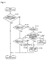
- FIG. 8 is a flowchart illustrating process steps of the data slice control method according to the fifth embodiment.
- FIG. 9 is a flowchart illustrating process steps of the data slice control method according to the sixth embodiment.
- FIG. 10 is a flowchart illustrating process steps of the data slice control method according to the seventh embodiment
- FIG. 11 is a flowchart illustrating the contents of a slice level control process that is one of the process steps of the data slice control method according to the seventh embodiment.
- FIG. 12 is a flowchart illustrating process steps of the data slice control method according to the eighth embodiment.
- FIG. 13 is a flowchart illustrating the contents of a slice level control process that is one of the process steps of the data slice control method according to the eighth embodiment.
- FIG. 14 is a block diagram illustrating the construction of a conventional data slice control device.
- FIG. 15 is a table illustrating various types of telecasts for explaining the conventional data slice control device.
- FIG. 1 is a block diagram illustrating the construction of the data slice control device according to the first embodiment.
- a video signal input terminal 101 receives an analog video signal S 101 in which telecast data are superposed in a vertical blanking period.
- An A/D converter 102 samples the analog video signal S 101 with a predetermined sampling clock fs (MHz) to convert the analog video signal S 101 into a digital video signal S 102 , and outputs the digital video signal S 102 to a low-pass filter (LPF) 103 .
- a predetermined sampling clock fs MHz
- LPF low-pass filter
- the LPF 103 subjects the inputted digital video signal S 102 to noise removal, and outputs the noise-removed digital video signal S 103 to a maximum value detection circuit 104 , a minimum value detection circuit 105 , a monotone increase detection circuit 106 , a monotone decrease detection circuit 107 , and a binarization circuit 114 .
- a sync separation circuit 119 separates the inputted digital video signal S 102 into a horizontal sync signal S 119 a and a vertical sync signal S 119 b , and outputs these signals to a clock run-in (CRI) period setting circuit 118 .
- the horizontal sync signal S 119 a and the vertical sync signal S 119 b are used for setting a position of a CRI period.
- a CRI period setting circuit 118 generates a CRI period setting signal S 118 for setting a CRI period of the telecast data superimposed in the digital video signal S 102 , on the basis of the vertical sync signal S 119 b and the horizontal sync signal S 119 a , and outputs the CRI period setting signal S 118 to the monotone increase detection circuit 106 , the monotone decrease detection circuit 107 , and a counter 108 .
- the monotone increase detection circuit 106 detects whether the amplitude values of the digital data at continuous three or more sampling points monotonously increase or not, on the basis of the CRI period setting signal S 118 and the noise-removed digital video signal S 103 .
- the monotone increase detection circuit 106 detects the monotone increase, it outputs a monotone increase detection signal S 106 to the maximum value detection circuit 104 , the minimum value detection circuit 105 , the counter 108 , and a CRI period determination circuit 112 .
- the monotone decrease detection circuit 107 detects whether the amplitude values of the digital data at continuous three or more sampling points monotonously decrease or not, on the basis of the CRI period setting signal S 118 and the noise-removed digital video signal S 103 .
- the monotone decrease detection circuit 107 detects the monotone decrease, it outputs a monotone decrease detection signal S 107 to a data holding circuit 110 .
- the maximum value detection circuit 104 detects a maximum value S 104 of the amplitudes of the digital data within the period during which the monotone increase is detected, on the basis of the monotone increase detection signal S 106 and the noise-removed digital video signal S 103 , and outputs the maximum value S 104 to a slice level calculation circuit 113 .
- the minimum value detection circuit 105 detects a minimum value S 105 of the amplitudes of the digital data within the period during which the monotone increase is detected, on the basis of the monotone increase detection signal S 106 and the noise-removed digital video signal S 103 , and outputs the minimum value S 105 to the slice level calculation circuit 113 .
- the counter 108 receives the CRI period setting signal S 118 and the monotone increase detection signal S 106 , and performs counting with the sampling clock during the period in which the CRI period setting signal S 118 is effective while resetting the count at the timing when the monotone increase detection signal S 106 becomes “H”, and outputs the result of counting as a count value S 108 to the data holding circuit 110 and the CRI period determination circuit 112 .
- the data holding circuit 110 receives the count value S 108 and the monotone decrease detection signal S 107 , and loads the count value S 100 at the timing when the monotone decrease detection signal S 107 becomes “H”, and simultaneously, holds the count value until the next monotone decrease detection signal S 107 is generated, and outputs the count value as a monotone increase monotone decrease interval value S 110 to the CRI period determination circuit 112 .
- a telecast mode storage table 111 contains telecast mode data which are indicated by the ratios between the transmission clocks of the respective telecast modes shown in FIG. 15 and the sampling clock, and outputs various telecast mode data S 111 to the CRI period determination circuit 112 .
- the CRI period determination circuit 112 determines as to whether the data signal is within the CRI period or not, on the basis of the monotone increase detection signal S 106 , the count value S 108 , the monotone increase monotone decrease interval value S 110 , and the various telecast mode data S 111 . When the CRI period determination circuit 112 determines that the data signal is within the CRI period, it outputs a CRI period determination signal S 112 to the slice level calculation circuit 113 .
- the slice level calculation circuit 113 calculates a slice level S 113 by averaging the maximum value S 104 and the minimum value S 105 which are detected within the period that is judged as the CRI period, on the basis of the maximum value 104 , the minimum value S 105 , and the CRI period determination signal S 112 , and outputs the slice level S 113 to the binarization circuit 114 .
- the binarization circuit 114 converts the noise-removed video signal S 103 into a binarization signal S 114 comprising 0 and 1 by the slice level S 113 , and outputs the binarized signal S 114 to a sampling circuit 115 .
- the sampling circuit 115 samples the binarized signal S 114 that is obtained by the binarization circuit 114 , at predetermined sampling intervals according to the type of the telecast mode, and outputs the sampled data S 115 to a decoding circuit 116 .
- the decoding circuit 116 converts the serial sampled data S 115 into a parallel signal, and subjects the parallel signal to a decoding process according to the type of the telecast, such as error correction, and thereafter, outputs the decoded data S 116 through an output terminal 117 to the outside.
- FIGS. 2( a )- 2 ( k ) are timing charts for explaining the operation of the data slice control device according to the first embodiment.
- 2 ( a ) shows the analog video signal S 101
- 2 ( b ) shows the horizontal sync signal S 119 a
- 2 ( c ) shows the CRI period setting signal S 111
- 2 ( d ) shows the monotone increase detection signal S 106
- 2 ( e ) shows the monotone decrease detection signal S 107
- 2 ( f ) shows the counter value S 108
- 2 ( g ) shows the monotone increase monotone decrease interval value S 110
- 2 ( h ) shows the maximum value S 104
- 2 ( i ) shows the minimum value S 105
- 2 ( j ) shows the CRI period determination signal S 112
- 2 ( k ) shows the slice level S 113 .
- the analog video signal S 101 supplied from the video signal input terminal 101 includes such as a horizontal sync signal, a burst signal, CRI data, and framing code data indicating the type of telecast or the like.
- black dots indicate the points sampled by the sampling clock. It is assumed that, in this first embodiment, the analog video signal S 102 is sampled at a sampling clock that is twice as high as the transmission clock.
- the sync separation circuit 119 separates the horizontal sync signal S 119 a as shown in FIG. 2( b ) from the digital video signal S 102 that is obtained by digitizing the analog video signal S 101 with the A/D converter 102 .
- the CRI period setting circuit 118 At time T 2 , the CRI period setting circuit 118 generates a CRI period setting signal S 118 for setting a CRI period, which is shown in FIG. 2( c ), on the basis of the horizontal sync signal S 119 a .
- the CRI period setting signal S 118 is not necessarily set so as to precisely include only the CRI period, and it may include a framing code period besides the CRI period.
- the monotone increase detection circuit 106 At times T 3 , T 5 , T 7 , T 9 , T 11 , and T 13 , the monotone increase detection circuit 106 generates a monotone increase detection signal S 106 shown in FIG. 2( d ) on the basis of the noise-removed digital video signal S 103 and the CRI period setting signal S 118 shown in FIG. 2( c ).
- the monotone increase detection circuit 106 changes the monotone increase detection signal S 106 to “H”, when the CRI period setting signal S 118 is “H”, and the amplitude value at the sampling point of the digital video signal at time T 3 is larger than the amplitude value at the sampling point which is one sampling point before that at time T 3 and smaller than the amplitude value at the sampling point which is one sampling point after that at time T 3 , i.e., when it is detected that the amplitude values at three or more consecutive sampling points monotonously increase.
- the monotone increase detection signal S 106 is changed to “H” when it is detected that the amplitude values at three consecutive sampling points monotonously increase.
- the monotone decrease detection circuit 107 At times T 4 , T 6 , T 8 , T 10 , T 12 , and T 14 , the monotone decrease detection circuit 107 generates a monotone decrease detection signal S 107 shown in FIG. 2( e ) on the basis of the noise-removed digital video signal S 103 and the CRI period setting signal S 118 shown in FIG. 2( c ).
- the monotone decrease detection circuit 107 changes the monotone decrease detection signal S 107 to “H”, when the CRI period setting signal S 118 is “H”, and the amplitude value at the sampling point of the digital video signal at time T 4 is smaller than the amplitude value at the sampling point which is one sampling point before that at time T 4 and larger than the amplitude value at the sampling point which is one sampling point after that at time T 4 , i.e., when it is detected that the amplitude values at three or more consecutive sampling points monotonously decrease.
- the monotone decrease detection signal S 107 is changed to “H” when it is detected that the amplitude values at three consecutive sampling points monotonously decrease.
- the counter 108 performs counting only when the CRI period setting signal S 118 shown in FIG. 2( c ) is “H”, and resets the count at the timing when the monotone increase detection signal S 106 shown in FIG. 2( d ) becomes “H”. That is, the count value of the counter 108 changes as shown in FIG. 2( f ).
- the data holding circuit 110 loads the count values shown in FIG. 2( f ) at the timing when the monotone decrease detection signal S 107 shown in FIG. 2( e ) becomes “H”, and holds the count values as the monotone increase monotone decrease interval data shown in FIG. 2( g ).
- the maximum value detection circuit 104 detects the maximum value S 104 of the amplitude values of the digital data as shown in FIG. 2( h ) from the noise-removed digital video signal S 103 . However, the maximum value detection circuit 104 detects the maximum value during the period from when the monotone increase detection signal S 106 shown in FIG. 2( d ) becomes “H” to when the next monotone increase detection signal S 106 becomes “H”. That is, when the monotone increase detection signal S 106 becomes “H”, the maximum value up to now is cleared, and detection of a maximum value is again carried out.
- the minimum value detection circuit 105 detects the minimum value S 105 of the amplitude values of the digital data as shown in FIG. 2( i ) from the noise-removed digital video signal S 103 . However, the minimum value detection circuit 104 detects the minimum value during the period from when the monotone increase detection signal S 106 shown in FIG. 2( d ) becomes “H” to when the next monotone increase detection signal S 106 becomes “H”. That is, when the monotone increase detection signal S 106 becomes “H”, the minimum value up to now is cleared, and detection of a minimum value is again carried out.
- the CRI period determination circuit 112 generates a CRI period determination signal S 112 shown in FIG. 2( j ) on the basis of the count value S 108 obtained from the counter 108 , the monotone increase detection signal S 106 obtained from the monotone increase detection circuit 106 , and the monotone increase monotone decrease interval value S 110 obtained from the data holding circuit 110 .
- the CRI period is equivalent to 4 sampling points.
- the monotone increase detection signal S 106 becomes “H”, and the count value S 108 at this time is 0 as shown in FIG.
- the monotone increase monotone decrease interval value S 110 is also 0 as shown in FIG. 2( g ).
- the count value becomes 3 which is obtained by subtracting 1 from 4 that corresponds to the CRI period.
- the monotone increase monotone decrease interval value becomes 1 which is obtained by subtracting 1 from 2 that corresponds to the period of the transmission clock.
- the count value S 108 at the timing when the monotone increase detection signal S 106 becomes “H” is 3 as shown in FIG.
- the monotone increase monotone decrease interval value S 110 is 1 as shown in FIG. 2( g ).
- a CRI period determination signal S 112 is generated as shown in FIG. 2( j ). That is, the CRI period determination signal S 112 becomes “H”.
- a CRI period determination signal S 112 is generated at times T 7 , T 9 , and T 11 .
- the monotone increase detection signal S 106 becomes “H”
- the count value S 108 at this time becomes 9 as shown in FIG. 2( f )
- the monotone increase monotone decrease interval value S 110 becomes 4 as shown in FIG. 2( g ). Therefore, these values are determined as abnormal, and no CRI period determination signal S 112 is generated.
- the slice level calculation circuit 113 calculates a slice level S 113 using the maximum value S 104 , the minimum value S 105 , and the CRI period determination signal S 112 .
- the slice level calculation circuit 113 loads the maximum value S 104 and the minimum value S 105 at the timing when the CRI period determination signal S 112 shown in FIG. 2( j ) becomes “H”, and outputs the average of the maximum value S 104 and the minimum value S 105 at this time, as a slice level S 113 shown in FIG. 2( k ).
- the maximum value S 104 and the minimum value S 105 are successively detected as shown in FIG. 2( h ) and FIG. 2( i ), respectively, during the period from time T 11 to time T 12 , but no CRI period determination signal S 112 is generated. Therefore, no slice level S 113 is calculated from the maximum value S 104 and the minimum value S 105 which are detected at this timing, as shown in FIG. 2( k ).
- the data slice control device provides the following effects. Since the telecast signals typified by a teletext signal is superimposed in the vertical blanking period of the television signal, the horizontal sync signal S 119 a that is separated by the sync separation circuit 119 is disturbed by such as a macrovision signal of a copy guard signal that is superimposed in the vertical blanking period. Therefore, the horizontal sync signal S 119 a in the line where the teletext signal is superimposed is not always separated in the position shown in FIG. 2( b ). Therefore, it is considerably difficult to set the CRI period setting signal S 118 , which is generated with reference to the horizontal sync signal S 119 a , so as to include only the CRI period.
- the data slice control device calculates the monotone increase point and monotone decrease point of data, the monotone increase interval value from the monotone increase point to the next monotone increase point, and the monotone increase monotone decrease interval value from the monotone increase point to the monotone decrease point, and determines a CRI period from the monotone increase interval value and the monotone increase monotone decrease interval value, and then calculates a slice level only in the determined period. Therefore, even when the horizontal sync signal S 119 a is disturbed, an accurate slice level can be detected.
- the CRI detection is carried out on the basis of the type of the telecast mode and the frequency of the sampling clock, only the sampling clock should be determined to perform accurate calculation of slice levels corresponding to not only the teletext employed in Europe but also VPS, WSS, multiplex telecast employed in Japan, electron programming guide (EPG), and closed caption employed in U.S.A., i.e., the data slice control device according to the first embodiment is adaptable to the telecast modes employed all over the world.
- EPG electron programming guide
- FIG. 3 is a block diagram illustrating the construction of the data slice control device according to the second embodiment.
- the data slice control device according to the second embodiment is provided with a determination signal counter 320 , an accumulation circuit 321 , and a data selection circuit 322 , in addition to the constituents of the data slice control device according to the first embodiment.
- the constituents other than mentioned above are identical to those described for the first embodiment, and therefore, repeated description is not necessary.
- the determination signal counter 320 counts the CRI period determination signal S 312 outputted from the CRI period determination circuit 312 , and outputs the result of counting as a determination signal count value S 320 during the CRI period to the data selection circuit 322 .
- the accumulation circuit 321 accumulates the slice level S 313 calculated by the slice level calculation circuit 313 , and outputs the result as an accumulated value S 321 to the data selection circuit 322 .
- the data selection circuit 322 selects an optimum slice level on the basis of the CRI period determination signal count value S 320 and the accumulated value S 321 , and outputs the selected slice level S 322 to the binarization circuit 314 .
- FIGS. 4( a )- 4 ( k ) are timing charts for explaining the operation of the data slice control device according to the second embodiment.
- 4 ( a ) shows an analog video signal S 301
- 4 ( b ) shows a horizontal sync signal S 319 a
- 4 ( c ) shows a CRI period setting signal S 318
- 4 ( d ) shows the monotone increase detection signal S 306
- 4 ( e ) shows a monotone decrease detection signal S 307
- 4 ( f ) shows a counter value S 308
- 4 ( g ) shows a monotone increase monotone decrease interval value S 310
- 4 ( h ) shows a CRI period determination signal S 312
- 4 ( i ) shows a slice level S 313
- 4 ( j ) shows a determination signal count value S 320
- 4 ( k ) shows an accumulated value S 321
- 4 ( l ) shows a selected slice level S 322 .
- the analog video signal S 301 inputted to the video signal input terminal 301 includes such as a horizontal sync signal, a burst signal, CRI data, and framing code data that shows the type of telecast or the like, as shown in FIG. 4( a ).
- black dots indicate the points sampled by the sampling clock, and the sampling clock is twice as high as the transmission clock.
- the sync separation circuit 319 separates the horizontal sync signal S 319 a as shown in FIG. 4( b ) from the digital video signal S 302 that is obtained by digitizing the analog video signal S 301 using the A/D converter 302 .
- the CRI period setting circuit 318 At time T 2 , the CRI period setting circuit 318 generates a CRI period setting signal S 318 for setting the CRI period shown in FIG. 4( c ), on the basis of the horizontal sync signal S 319 a .
- the CRI period setting signal S 318 is not necessarily set so as to precisely include only the CRI period, and it may include a framing code period besides the CRI period.
- the monotone increase detection circuit 306 At times T 3 , T 5 , T 7 , T 9 , T 11 , and T 13 , the monotone increase detection circuit 306 generates a monotone increase detection signal S 306 shown in FIG. 4( d ) on the basis of the noise-removed digital video signal S 303 and the CRI period setting signal S 318 shown in FIG. 4( c ).
- the method of generating the monotone increase detection signal S 306 is identical to the method of generating the monotone increase detection signal S 106 according to the first embodiment, and therefore, repeated description is not necessary.
- the monotone decrease detection circuit 307 At times T 4 , T 6 , T 8 , T 10 , T 12 , and T 14 , the monotone decrease detection circuit 307 generates a monotone decrease detection signal S 307 shown in FIG. 4( e ) on the basis of the noise-removed digital video signal S 303 and the CRI period setting signal S 318 shown in FIG. 4( c ).
- the method of generating the monotone decrease detection signal S 307 is identical to the method of generating the monotone increase detection signal S 107 according to the first embodiment, and therefore, repeated description is not necessary.
- the counter 308 operates only when the CRI period setting signal S 318 shown in FIG. 4( c ) is “H”, and resets the count at the timing when the monotone increase detection signal S 306 shown in FIG. 4( d ) becomes “H”. That is, the count value of the counter 308 changes as shown in FIG. 4( f ).
- the data holding circuit 310 loads the count value shown in FIG. 4( f ) at the timing when the monotone decrease detection signal S 307 shown in FIG. 4( e ) becomes “H”, and holds the count value as the monotone increase monotone decrease interval data shown in FIG. 4( g ).
- the maximum value detection circuit 304 detects the maximum value S 304 of the amplitude values of the noise-removed digital video signal S 303 . However, the maximum value detection circuit 304 detects the maximum value during a period from when the monotone increase detection signal S 306 shown in FIG. 4( d ) becomes “H” to when the next monotone increase detection signal S 306 becomes “H”. That is, when the monotone increase detection signal S 306 becomes “H”, the maximum value up to slow is cleared, and detection of a maximum value is again carried out. Since detection of the maximum value S 304 by the maximum value detection circuit 304 is carried out in the same method for detecting the maximum value S 104 according to the first embodiment, it is omitted in FIG. 4 .
- the minimum value detection circuit 305 detects the minimum value S 305 of the amplitude values of the noise-removed digital video signal S 303 . However, the minimum value detection circuit 305 detects the minimum value during a period from when the monotone increase detection signal S 306 shown in FIG. 4( d ) becomes “H” to when the next monotone increase detection signal S 306 becomes “H”. That is, when the monotone increase detection signal S 306 becomes “H”, the minimum value up to now is cleared, and detection of a minimum value is again carried out. Since detection of the minimum value S 305 by the minimum value detection circuit 305 is carried out in the same method for detecting the minimum value S 105 according to the first embodiment, it is omitted in FIG. 4 .
- the CRI period determination circuit 312 generates a CRI period determination signal S 312 shown in FIG. 4( h ) on the basis of the count value S 308 obtained from the counter 308 , the monotone increase detection signal S 306 obtained from the monotone increase detection circuit 306 , and the monotone increase monotone decrease interval value S 310 obtained from the data holding circuit 310 .
- the CRI period corresponds to 4 sampling points.
- the monotone increase detection signal S 306 becomes “H”, and the count value S 308 at this time is 0 as shown in FIG.
- the monotone increase monotone decrease interval value S 310 is also 0 as shown in FIG. 4( g ).
- the count value becomes 3 which is obtained by subtracting 1 from 4 that corresponds to the CRI period.
- the monotone increase monotone decrease interval value becomes 1 which is obtained by subtracting 1 from 2 that corresponds to the period of the transmission clock.
- the count value S 308 at the timing when the monotone increase detection signal S 306 is “H” is 3 as shown in FIG.
- the monotone increase monotone decrease interval value S 310 is 1 as shown in FIG. 4( g ).
- a CRI period determination signal S 312 is generated as shown in FIG. 4( j ). That is, the CRI period determination signal S 312 becomes “H”.
- a CRI period determination signal S 312 is generated at times T 7 , T 9 , and T 11 .
- the monotone increase detection signal S 306 becomes “H” at time T 13
- the count value S 308 at this time becomes 9 as shown in FIG. 4( f )
- the monotone increase monotone decrease interval value S 310 becomes 4 as shown in FIG. 4( g ). Therefore, these values are determined as abnormal, and no CRI period determination signal S 312 is generated.
- the slice level calculation circuit 313 calculates a slice level S 313 using the maximum value S 304 , the minimum value S 305 , and the CRI period determination signal S 312 .
- the slice level calculation circuit 313 loads the maximum value S 304 and the minimum value S 305 at the timing when the CRI period determination signal S 312 shown in FIG. 4( h ) becomes “H”, and outputs the average of the maximum value S 304 and the minimum value S 305 at this time as a slice level S 313 shown in FIG. 4( i ).
- the determination signal counter 320 performs counting only when the CRI period determination signal S 312 is “H”, and the counting result changes as the determination signal count value S 320 shown in FIG. 4( j ).
- the accumulation circuit 321 successively accumulates the slice level S 313 shown in FIG. 4( i ) to obtain an accumulated value S 321 as shown in FIG. 4( k ).
- the data selection circuit 322 calculates a selected slice level S 322 on the basis of the accumulated value S 321 obtained from the accumulation circuit 321 and the determination signal count value S 320 obtained by the determination signal counter 320 .
- the CRI corresponds to 8 periods at maximum, and therefore, the determination signal count value S 320 is controlled so as not to exceed 8.
- the accumulated value S 321 is divided by the determination signal count value S 320 , and the result is used as a selected slice level S 322 . In this second embodiment, however, in order to prevent an increase in the circuit scale, division is not carried out, and a selected slice level S 322 is obtained using only shift operation.
- the ACMD 1 is selected when the determination signal count value is 1, the ACMD 2 is selected when the count value is 2 or 3, the ACMD 3 is selected when the count value is 4, 5, 6, or 7, and the ACMD 4 is selected when the count value is 8 or more.
- the determination signal count value S 320 when the determination signal count value S 320 is 1, the value 115 of the accumulated value S 321 is selected as it is.
- the determination signal count value S 320 is 2 or 3
- the value 102 that is obtained by shifting the value 205 of the accumulated value S 321 by one bit to the right, i.e., by dividing the value 205 with 2, is selected.
- the determination signal count value S 320 becomes 4
- the value 103 obtained by shifting the value 415 of the accumulated value S 321 by two bits to the right, i.e., by dividing the value 415 by 4 is selected.
- the count value is successively selected by the above-mentioned method.
- the slice level and the timing when the CRI period determination signal becomes “H” are counted, and a slice level at which the CRI does not exceed the maximum period is selected. Therefore, as shown in FIG. 4( a ), even when the signal is disturbed due to ghosts or noises and thereby the maximum value becomes larger or smaller than the usual maximum value during the CRI period or the framing code period, it is possible to calculate an accurate slice level while reducing the adverse effects of ghosts and noise, by calculating slice levels only in the CRI period including the same frequency component, and taking the average of the slice levels.
- the data slice control device according to the first embodiment even when the horizontal sync signal S 119 a is disturbed, an accurate slice level can be detected. Further, the data slice control device according to the second embodiment is adaptable to the telecast modes employed all over the world.
- the above-mentioned method is employed for slice level selection to reduce the circuit scale.
- the accumulated value S 321 may be simply divided by the determination signal count value S 320 to use the result as a selected slice level.
- FIG. 5 is a block diagram illustrating the construction of the data slice control device according to the third embodiment.
- a video signal input terminal 501 receives an analog video signal S 501 in which telecast data are superposed in a vertical blanking period.
- An A/D converter 502 samples the analog video signal S 501 at a predetermined sampling clock fs (MHz) to convert the analog video signal S 501 into a digital video signal S 502 , and outputs the digital video signal S 502 to a low-pass filter (LPF) 503 .
- LPF low-pass filter
- the LPF 503 subjects the inputted digital video signal S 502 to noise removal, and outputs the noise-removed digital video signal S 503 to a maximum value detection circuit 504 , a minimum value detection circuit 505 , a coring circuit 523 , and a binarization circuit 514 .
- a sync separation circuit 519 separates the inputted digital video signal S 502 into a horizontal sync signal S 519 a and a vertical sync signal S 519 b , and outputs these signals to a CRI period setting circuit 518 .
- the horizontal sync signal S 519 a and the vertical sync signal S 519 b are used for setting the position of the CRI period.
- the CRI period setting circuit 518 generates a CRI period setting signal S 518 for setting a CRI period of the telecast data that is superimposed on the digital video signal S 502 , on the basis of the vertical sync signal S 519 b and the horizontal sync signal S 519 a , and outputs the CRI period setting signal S 518 to a masking circuit 524 and a counter 508 .
- the coring circuit 523 subjects the noise-removed digital video signal S 503 to coring, and outputs coring data S 523 to the masking circuit 524 .
- the coring is a process in which 0 is output when the noise-removed digital video signal S 503 (data value) is smaller than a coring level CORLMTD, and a value obtained by subtracting the coring level CORLMTD from the data value of the digital video signal S 503 is output when the digital video signal S 503 is larger than the coring level CORLMTD.
- the masking circuit 524 performs masking to make the coring data S 523 ineffective during a period other than when the CRI period setting signal S 518 is effective, and outputs the result to a delay unit 525 and a judgement unit 530 .
- the masking is a process of setting the coring data S 523 to an arbitrary fixed value during the period when the CRI period setting signal S 518 is ineffective.
- the delay unit 525 delays the coring data S 524 that has been subjected to masking, by one sampling clock (1T), and outputs the data S 524 to a comparator 529 and a delay unit 526 .
- the delay unit 526 delays the data S 525 that has been 1T-delayed by the delay unit 525 , by another 1T, and outputs the data S 525 to an adder 527 and the judgement unit 530 .
- the adder 527 adds the masking-processed coring data S 524 and the data S 526 that has been obtained by 2T-delaying the masking-processed coring data, and outputs the sum to a bit shifting unit 528 .
- the bit shifting unit 528 shifts the data S 527 obtained by the adder 527 by one bit to the right, and outputs the data to the comparator 529 .
- the one-bit right shifting halves the added data S 527 .
- the comparator 529 compares the 1T-delayed data S 525 with the one-bit right shifted data S 528 .
- the comparator 529 checks whether or not the one-bit right shifted data S 528 exists between a value that is obtained by subtracting a threshold value ⁇ from the 1T-delayed data S 525 and a value that is obtained by adding the threshold value ⁇ to the 1T-delayed data S 525 , and outputs a comparison result signal S 529 as a signal that becomes effective only when the data S 528 exists, to the masking circuits 531 and 532 .
- the judgement unit 530 judges that the amplitude values at the sampling points of the digital data monotonously increase, when the masking-processed coring data S 524 is larger than a value that is obtained by adding an arbitrary value ⁇ to the 2T-delayed data S 526 , and generates a monotone increase signal S 530 a to be output to the masking circuit 531 .
- the judgement unit 530 judges that the amplitude values of the digital data monotonously decrease, and generates a monotone decrease signal S 530 b to be output to the masking circuit 532 .
- the masking circuit 531 receives the monotone increase signal S 530 a and the comparison result signal S 529 , and generates a monotone increase detection signal S 531 when both of these signals are effective, and outputs the signal S 531 to the counter S 508 , the maximum value detection circuit 504 , the minimum value detection circuit 505 , and the CRI period determination circuit 512 .
- the masking circuit 532 receives the monotone decrease signal S 530 b and the comparison result signal S 529 , and generates a monotone decrease detection signal S 532 when both of these signals are effective, and outputs the signal S 532 to the data holding circuit 510 .
- the maximum value detection circuit 504 detects a maximum value S 504 the amplitude values of the digital data within the period during which monotone increase is detected, on the basis of the monotone increase detection signal S 531 and the noise-removed digital video signal S 503 , and outputs the maximum value S 504 to a slice level calculation circuit 513 .
- the minimum value detection circuit 505 detects a minimum value S 505 of the amplitude values of the digital data within the period during which monotone increase is detected, on the basis of the monotone increase detection signal S 531 and the noise-removed digital video signal S 503 , and outputs the minimum value S 505 to the slice level calculation circuit 513 .
- the counter 508 receives the CRI period setting signal S 518 and the monotone increase detection signal S 531 , and performs counting with the sampling clock during the period in which the CRI period setting signal S 518 is effective, while resetting the count at the timing when the monotone increase detection signal S 531 becomes “H”, and outputs the result of counting as a count value S 508 to the data holding circuit 510 and the CRI period determination circuit 512 .
- the data holding circuit 510 receives the count value S 508 and the monotone decrease detection signal S 532 , and loads the count value S 508 at the timing when the monotone decrease detection signal S 532 becomes “H”, and holds the data until the next monotone decrease detection signal S 532 is generated (until the next timing when the monotone decrease detection signal S 532 becomes “H”), and outputs a monotone increase monotone decrease interval value S 510 to the CRI period determination circuit 512 .
- a telecast mode storage table 511 contains telecast mode data which are indicated by the ratios between the transmission clocks of the various telecast modes shown in FIG. 15 and the sampling clock, and outputs the various telecast mode data S 511 to the CRI period determination circuit S 512 .
- the CRI period determination circuit 512 determines whether the data signal is within the CRI period or not, on the basis of the monotone increase detection signal S 531 , the count value S 508 , the monotone increase monotone decrease interval value S 510 , and the various telecast mode data S 111 . When the CRI period determination circuit 512 determines that the data signal is within the CRI period, it outputs a CRI period determination signal S 512 to the slice level calculation circuit 513 .
- the slice level calculation circuit 513 averages the maximum value S 504 and the minimum value S 505 which are detected during the period determined as the CRI period, on the basis of the maximum value S 504 , the minimum value S 505 , and the CRI period determination signal S 512 , thereby to calculate a slice level S 513 , and outputs the slice level S 513 to the binarization circuit 514 .
- the binarization circuit 514 converts the noise-removed digital video signal S 503 into a binarized signal S 514 comprising 0 and 1 by the slice level S 513 , and outputs the binarized signal S 514 to a sampling circuit 515 .
- the sampling circuit 515 samples the binarized signal S 514 that is outputted from the binarization circuit 514 , at predetermined sampling intervals according to the type of the telecast mode, and outputs the sampled data S 515 to a decoding circuit 516 .
- the decoding circuit 516 converts the serial sampled data S 515 into a parallel signal, and subjects the data S 515 to a decoding process according to the type of the telecast, such as error detection, and then outputs the decoded data S 516 through an output terminal 517 to the outside.
- the data control device provides the following effects.
- the data superimposed on the video signal is telecast data
- the telecast data exists at a level higher than the pedestal level of the video signal. Therefore, it is possible to reduce the adverse effects of noises lower than the pedestal level, by performing coring on the data signal using the coring circuit 523 .
- monotone increase detection and monotone decrease detection are carried out at the continuous three sampling points, and further, inclinations of monotone increase and monotone decrease are calculated and determined using the comparator 529 and the judgement unit 530 . Therefore, it is possible to perform more accurate monotone increase detection and monotone decrease detection while reducing adverse effects of noises or the like. As a result, the slice level to be calculated in the subsequent stage becomes to have higher accuracy.
- the data slice control device like the data slice control device according to the first embodiment, even when the horizontal sync signal is disturbed, an accurate slice level can be detected. Furthermore, the data slice control device according to the third embodiment is adaptable to the telecast modes employed all over the world.
- FIG. 6 is a block diagram illustrating the construction of the data slice control device according to the fourth embodiment.
- a video signal input terminal 601 receives an analog video signal S 601 in which telecast data are superposed in a vertical blanking period.
- An A/D converter 602 samples the analog video signal S 601 at a predetermined sampling clock fs (MHz) to convert the analog video signal S 601 into a digital video signal S 602 , and outputs the digital video signal S 602 to a low-pass filter (LPF) 603 .
- a predetermined sampling clock fs MHz
- LPF low-pass filter
- the LPF 603 subjects the inputted digital video signal S 602 to noise removal, and outputs the noise-removed digital video signal S 603 to a maximum value detection circuit 604 , a minimum value detection circuit 605 , a coring circuit 623 , and a binarization circuit 614 .
- a sync separation circuit 619 separates the inputted digital video signal S 602 into a horizontal sync signal S 619 a and a vertical sync signal S 619 b , and outputs these signals to a CRI period setting circuit 618 .
- the horizontal sync signal S 619 a and the vertical sync signal S 619 b are used for setting the position of the CRI period or the like.
- the CRI period setting circuit 618 generates a CRI period setting signal S 618 for setting a CRI period of the telecast data that is superimposed on the digital video signal S 602 , on the basis of the vertical sync signal S 619 b and the horizontal sync signal S 619 a , and outputs the CRI period setting signal S 618 to a masking circuit 624 and a counter 608 .
- the coring circuit 623 subjects the noise-removed digital video signal S 603 to coring, and outputs coring data S 623 to the masking circuit 624 .
- the coring is a process in which 0 is output when the noise-removed digital video signal S 603 (data value) is smaller than a coring level CORLMTD, and a value obtained by subtracting the coring level CORLMTD from the data value of the digital video signal S 603 is output when the digital video signal S 603 is larger than the coring level CORLMTD.
- the masking circlet 624 performs masking to make the coring data S 623 ineffective during a period other than when the CRI period setting signal S 618 is effective, and outputs the result to a delay unit 625 and a judgement unit 630 .
- the masking is a process of setting the coring data S 623 to an arbitrary fixed value during the period when the CRI period setting signal S 618 is ineffective.
- the delay unit 625 delays the coring data S 624 that has been subjected to masking, by one sampling clock (1T), and outputs the data S 624 to a comparator 629 and a delay unit 626 .
- the delay unit 626 delays the data S 625 that has been 1T-delayed by the delay unit 625 , by another 1T, and outputs the data S 625 to an adder 627 and the judgement unit 630 .
- This data is 2T-delayed with respect to the coring data S 624 that has been subjected to masking.
- the adder 627 adds the masking-processed coring data S 624 and the data S 626 that has been obtained by 2T-delaying the masking-processed coring data, and outputs the sum S 627 to a bit shifting unit 628 .
- the bit shifting unit 628 shifts the data S 627 obtained by the adder 627 by one bit to the right, and outputs the data to the comparator 629 .
- the one-bit right shifting halves the added data S 627 .
- the comparator 629 compares the 1T-delayed data S 625 with the one-bit right shifted data S 628 , and outputs the result to masking circuits 631 and 632 .
- the comparator 629 checks whether or not the one-bit right shifted data S 628 exists between a value that is obtained by subtracting a threshold value ⁇ from the 1T-delayed data S 625 and a value that is obtained by adding the threshold value ⁇ to the 1T-delayed data S 625 , and outputs a comparison result signal S 629 as a signal that becomes effective only when the data S 628 exists.
- the judgement unit 630 judges that the amplitude values at the sampling points of the digital data monotonously increase, when the masking-processed coring data S 624 is larger than a value that is obtained by adding an arbitrary value ⁇ to the 2T-delayed data S 626 , and generates a monotone increase signal S 630 a to be output to the masking circuit 631 .
- the judgement unit 630 judges that the amplitude values at the sampling points of the digital data monotonously decrease, and generates a monotone decrease signal S 630 b to be output to the masking circuit 632 .
- the masking circuit 631 receives the monotone increase signal S 630 a and the comparison result signal S 629 , and generates a monotone increase detection signal S 631 when both of these signals are effective, and outputs the signal S 631 to the counter S 608 , the maximum value detection circuit 604 , the minimum value detection circuit 605 , and the CRI period determination circuit 612 .
- the masking circuit 632 receives the monotone decrease signal S 630 b and the comparison result signal S 629 , and generates a monotone decrease detection signal S 632 when both of these signals are effective, and outputs the signal S 632 to the data holding circuit 610 .
- the maximum value detection circuit 604 detects a maximum value S 604 of the amplitude values of the digital data within the period during which monotone increase is detected, on the basis of the monotone increase detection signal S 631 and the noise-removed digital video signal S 603 , and outputs the maximum value S 604 to a slice level calculation circuit 613 .
- the minimum value detection circuit 605 detects a minimum value S 605 of the amplitude values of the digital data within the period during which monotone increase is detected, on the basis of the monotone increase detection signal S 631 and the noise-removed digital video signal S 603 , and outputs the minimum value S 605 to the slice level calculation circuit 613 .
- the counter 608 receives the CRI period setting signal S 618 and the monotone increase detection signal S 631 , and performs counting with the sampling clock during the period in which the CRI period setting signal S 618 is effective, while resetting the count at the timing when the monotone increase detection signal S 631 is “H”, and outputs the result of counting as a count value S 608 to the data holding circuit 610 and the CRI period determination circuit 612 .
- the data holding circuit 610 receives the count value S 608 and the monotone decrease detection signal S 632 , and loads the count value S 608 at the timing when the monotone decrease detection signal S 632 becomes “H”, and holds the data until the next monotone decrease detection signal S 632 is generated (until the next timing when the monotone decrease detection signal S 632 becomes “H”), and outputs a monotone increase monotone decrease interval value S 610 to the CRI period determination circuit 612 .
- a telecast mode storage table 611 contains telecast mode data which are indicated by the ratios between the transmission clocks of the various telecast modes shown in FIG. 15 and the sampling clock, and outputs the various telecast mode data S 611 to the CRI period determination circuit S 612 .
- the CRI period determination circuit 612 determines whether the data signal is within the CRI period or not, on the basis of the monotone increase detection signal S 631 , the count value S 608 , the monotone increase monotone decrease interval value S 610 , and the various telecast mode data S 611 . When the CRI period determination circuit 612 determines that the data signal is within the CRI period, it outputs a CRI period determination signal S 612 to the slice level calculation circuit 613 .
- the slice level-calculation circuit 613 averages the maximum value S 604 and the minimum value S 605 which are detected during the period that is determined as the CRI period, on the basis of the maximum value S 604 , the minimum value S 605 , and the CRI period determination signal S 612 , thereby to calculate a slice level S 613 , and outputs the slice level S 613 to an accumulation circuit 621 .
- a determination signal counter 620 counts the CRI period determination signal S 612 , and outputs the result of counting as a determination signal count value S 620 in the CRI period to a data selection circuit 622 .
- the accumulation circuit 621 accumulates the slice level S 613 calculated by the slice level calculation circuit 613 , and outputs the result of accumulation as an accumulated value S 621 to the data selection circuit 622 .
- the data selection circuit 622 selects an optimum slice level on the basis of the determination signal count value S 620 and the accumulated value S 621 during the CRI period, and outputs the selected slice level S 622 to the binarization circuit 614 . Since the method of calculating a selected slice level is identical to that described for the second embodiment, repeated description is not necessary.
- the binarization circuit 614 converts the noise-removed digital video signal S 603 into a binarized signal S 614 comprising 0 and 1 by the slice level S 613 , and outputs the binarized signal S 614 to a sampling circuit 615 .
- the sampling circuit 615 samples the binarized signal S 614 that is outputted from the binarization circuit 614 , at predetermined sampling intervals according to the type of the telecast mode, and outputs the sampled data S 615 to a decoding circuit 616 .
- the decoding circuit 616 converts the serial sampled data S 615 into a parallel signal, and subjects the data S 615 to a decoding process according to the type of the telecast, such as error detection, and then outputs the decoded data S 616 through an output terminal 617 to the outside.
- the data control device provides the following effects. That is, when the data superimposed in the video signal is telecast data, the telecast data exists at a level higher than the pedestal level of the video signal. Therefore, it is possible to reduce adverse effects of noises lower than the pedestal level, by subjecting the data signal to coring using the coring circuit 623 . Further, in this fourth embodiment, monotone increase detection and monotone decrease detection are carried out at the continuous three sampling points, and furthermore, inclinations of monotone increase and monotone decrease are calculated and determined using the comparator 629 and the judgement unit 630 . Therefore, it is possible to perform more accurate monotone increase detection and monotone decrease detection while reducing adverse effects of noises or the like.
- the slice level to be calculated in the subsequent stage becomes to have higher accuracy. Furthermore, the timing when the slice level and the CRI period determination signal are “H” is counted to select a slice level at which the CRI does not exceed the maximum cycle. Therefore, even when the signal is disturbed due to ghosts or noises and thereby the maximum value becomes larger or smaller than the usual maximum value during the CRI period or the framing code period, it is possible to obtain an accurate slice level while reducing the adverse effects of ghosts or noises, by calculating slice levels only in the CRI period including the same frequency component, and averaging the slice levels.
- the data slice control device like the data slice control device according to the first embodiment, even when the horizontal sync signal is disturbed, an accurate slice level can be detected. Further, the data slice control device according to the fourth embodiment is adaptable to the telecast modes employed all over the world.
- monotone increase detection and monotone decrease detection are carried out at three sampling points, monotone increase detection and monotone decrease detection may be carried out at four or more sampling points with the same effects as described above.
- the period during which a slice level is to be detected is set so as to include the CRI period
- the present invention is not restricted thereto.
- This period may be set so as to include periods other than the CRI period, such as a data period.
- sampling clock is set twice as high as the transmission clock
- present invention is not restricted thereto.
- the sampling clock may be set more than twice as high as the transmission clock with the same effects as mentioned above.
- the telecast signal employed in the first to fourth embodiments is a teletext signal
- the present invention is not restricted thereto. Even when a signal other than the teletext signal is employed, an accurate slice level can be calculated by detecting a CRI and calculating a slice level during the detected period.
- FIG. 7 is a block diagram illustrating the construction that realizes the data slice control method according to the fifth embodiment of the invention.
- a video signal input terminal 701 receives an analog video signal S 701 in which telecast data are superposed in a vertical blanking period.
- An A/D converter 702 samples the analog video signal S 701 at a predetermined sampling clock fs (MHz) to convert the analog video signal S 701 into a digital video signal S 702 , and outputs the digital video signal S 702 to a low-pass filter (LPF) 703 .
- a predetermined sampling clock fs MHz
- LPF low-pass filter
- the LPF 703 subjects the inputted digital video signal S 702 to noise removal, and outputs the noise-removed digital video signal S 703 to a RAM 741 and a binarization circuit 714 .
- a sync separation circuit 719 separates the inputted digital video signal S 702 into a horizontal sync signal S 719 a and a vertical sync signal S 719 b , and outputs these signals to a CRI period setting circuit 718 .
- the horizontal sync signal S 719 a and the vertical sync signal S 719 b are used for setting the position or the CRI period.
- the CRI period setting circuit 718 generates a CRI period setting signal S 718 for setting a CRI period of the telecast data that is superimposed on the digital video signal S 702 , on the basis of the vertical sync signal S 719 b and the horizontal sync signal S 719 a , and outputs the CRI period setting signal S 718 to a RAM address generation circuit 740 .
- the RAM address generation circuit 740 generates RAM addresses S 740 for writing the noise-removed digital video signal S 703 into the RAM 741 during a period when the CRI period setting signal S 718 is effective, and outputs the RAM addresses S 740 to the RAM 741 .
- the RAM 741 stores the noise-removed digital video signal S 703 on the basis of the RAM addresses obtained from the RAM address generation circuit 740 .
- a microcomputer 742 calculates an optimum slice level using the data which have been stored in the RAM 741 during only the period when the CRI period setting signal S 718 is effective, and outputs the slice level to the binarization circuit 714 the binarization circuit 714 converts the noise-removed digital video signal S 703 into a binarized signal S 714 comprising 0 and 1 by the slice level S 742 , and outputs the binarized signal S 714 to a sampling circuit 715 .
- the sampling circuit 715 samples the binarized signal S 714 at predetermined sampling intervals according to the type of the telecast mode, and outputs the sampled data S 715 to a decoding circuit 716 .
- the decoding circuit 716 converts the serial sampled data S 715 into a parallel signal, and subjects the data S 715 to a decoding process according to the type of the telecast, such as error detection, and then outputs the decoded data S 716 through an output terminal 717 to the outside.
- step S 801 an address i of the RAM 741 , a variable j, a maximum value detection variable MAX, and a minimum value detection variable MIN are initialized, and the process goes to step S 802 .
- step S 802 the RAM data RAM(i) stored in the address i is compared with the maximum value detection variable MAX, and the process goes to step S 803 when the RAM data RAM(i) stored in the address i is larger than the maximum value detection variable MAX. Otherwise, the process goes to step S 804 .
- step S 803 the maximum value detection variable MAX is changed to the RAM data RAM(i), and the process goes to step S 806 .
- step S 804 the RAM data RAM(i) stored in the address i is compared with the minimum value detection variable MIN, and the process goes to step S 805 when the RAM data RAM(i) stored in the address i is smaller than the minimum value detection variable MIN. Otherwise, the process goes to step S 806
- step S 805 the minimum value detection variable MIN is changed to the RAM data RAM(i), and the process goes to step S 806 .
- step S 806 the RAM data RAM(i) stored in the current RAM address i, the RAM data RAM(i ⁇ 1) stored in the RAM address i ⁇ 1, and the RAM data RAM(i+1) stored in the RAM address i+1 are compared, and the process goes to step S 807 when the sizes of these data, data values) are in the relationship of RAM(i ⁇ 1) ⁇ RAM(i) ⁇ RAM(i+1). Otherwise, the process goes to step S 812 .
- step S 807 the RAM address i is stored in a monotone increase detection address storage buffer INCADR(j), and the process goes to step S 808 .
- step S 808 judgement of monotone increase is carried out using the address value stored in the monotone increase detection address storage buffer INCADR(j), the address value stored in a monotone increase detection address storage buffer INCADR(j ⁇ 1), and CRI frequency data CRIFQ.
- the CRI frequency data CRIFQ can be obtained using the ratio between the sampling clock fs (MHz) and the transmission clock fchr (MHz) of the telecast data, i.e., it is calculated by 2fs/fchr.
- the RAM address j ⁇ 1 that is stored in the immediately preceding monotone increase detection address storage buffet INCADR(j ⁇ 1) is subtracted from the RAM address j that is stored in the current monotone increase detection address storage buffer INCADR(j), and it is checked whether the value is equal to the CRI frequency data CRIFQ or not.
- the RAM address j ⁇ 1 that is stored in the monotone increase detection address storage buffer INCADR(j ⁇ 1) is subtracted from the RAM address j that is stored in the current monotone decrease detection address storage buffer DECADR(j), and it is checked whether the value is equal to 1 ⁇ 2 of the CRI frequency data CRIFQ or not.
- the process goes to step S 809 . Otherwise, the process goes to step S 811 .
- step S 809 the slice level variable SLV is changed to the average of the maximum value detection variable MAX and the minimum value detection variable MIN, and the process goes to step S 811 .
- step S 811 the maximum value detection variable. MAX and the minimum value detection variable MIN are initialized, and the variable j is incremented, and then the process goes to step S 814 .
- step S 812 the RAM data RAM(i) stored in the current RAM address i, the RAM data RAM(i ⁇ 1) stored in the RAM address i ⁇ 1, and the RAM data RAM(i+1) stored in the RAM address i+1 are compared, and the process goes to step S 813 when the sizes of these data (data values) are in the relationship of RAM(i+1)>RAM(i)>RAM(i ⁇ 1). Otherwise, the process goes to step S 814 .
- step S 813 the RAM address i is stored in the monotone decrease detection address storage buffer DECADR(j), and the process goes to step S 814 .
- step S 814 it is checked whether the RAM address is a final address or not. When it is a final address, the process is ended. When it is not a final address, the process goes to step S 815 .
- step S 815 the RAM address i is incremented, and the process returns to step S 802 .
- the microcomputer 742 successively carries out steps S 802 to S 814 until the RAM address i becomes a final address.
- the data slice control method provides the following effects. Since the telecast signal represented by a teletext signal is superimposed on the vertical blanking period of a television signal, the horizontal sync signal S 719 a separated by the sync separation circuit 719 is disturbed due to a macrovision signal of a copy guard signal or the like that is superimposed on the vertical blanking period. Therefore, it is considerably difficult to set the CRI period setting signal S 718 , which is generated with reference to the horizontal sync signal S 719 a , so as to include only the CRI period.
- the range of the CRI period setting signal S 718 is increased so as to include the CRI period, and the CRI is automatically detected within the period indicated by the CRI period setting signal, whereby more accurate slice level can be detected.
- the data slice control device is adaptable to the telecast modes employed all over the world.
- FIG. 9 is a flowchart for explaining the contents of processing to be performed by the microcomputer 742 shown in FIG. 7 . Since the processes other than those shown in FIG. 9 are identical to those described for the fifth embodiment, repeated description is not necessary.
- step S 901 the address i of the RAM 741 , the variable j, the maximum value detection variable MAX, the minimum value detection variable MIN, the judgement result count variable JDCNT, and the slice level accumulation variable SLACMD are initialized, and the process goes to step S 902 .
- step S 902 the RAM data RAM(i) stored in the address i is compared with the maximum value detection variable MAX, and the process goes to step S 903 when the RAM data RAM(i) stored in the address i is larger than the maximum value detection variable MAX. Otherwise, the process goes to step S 904 .
- step S 903 the maximum value detection variable MAX is changed to the RAM data RAM(i), and the process goes to step S 906 .
- step S 904 the RAM data RAM(i) stored in the address i is compared with the minimum value detection variable MIN, and the process goes to step S 905 when the RAM data RAM(i) stored in the address i is smaller than the minimum value detection variable MIN. Otherwise, the process goes to step S 906 .
- step S 905 the minimum value detection variable MIN is changed to the RAM data RAM(i), and the process goes to step S 906 .
- step S 906 the RAM data RAM(i) stored in the current RAM address i, the RAM data RAM(i ⁇ 1) stored in the RAM address i ⁇ 1, and the RAM data RAM(i+1) stored in the RAM address i+1 are compared, and the process goes to step S 907 when the sizes of these data (data values) are in the relationship of RAM(i ⁇ 1) ⁇ RAM(i) ⁇ RAM(i+1). Otherwise, the process goes to step S 914 .
- step S 907 the RAM address i is stored in the monotone increase detection address storage buffer INCADR(j), and the process goes to step S 908 .
- step S 908 judgement of monotone increase is carried out using the address value stored in the monotone increase detection address storage buffer INCADR(j), the address value stored in the immediately preceding monotone increase detection address storage buffer INCADR(j ⁇ 1), and the CRI frequency data CRIFQ.
- the CRI frequency data CRIFQ can be obtained using the ratio between the sampling clock fs(MHz) and the transmission clock fchr(MHz) of the telecast data, i.e., it is calculated by 2fs/fchr.
- the RAM address j ⁇ 1 that is stored in the immediately preceding monotone increase detection address storage buffer INCADR(j ⁇ 1) is subtracted from the RAM address j that is stored in the current monotone increase detection address storage buffer INCADR(j), and it is checked whether the value is equal to the CRI frequency data CRIFQ or not.
- the RAM address j ⁇ 1 that is stored in the monotone increase detection address storage buffer INCADR(j ⁇ 1) is subtracted from the RAM address j that is stored in the current monotone decrease detection address storage buffer DECADR(j), and it is checked whether the value is equal to 1 ⁇ 2 or the CRI frequency data CRIFQ or not.
- the process goes to step S 909 . Otherwise, the process goes to step S 913 .
- step S 909 the judgement result count variable JDCNT is incremented, and the process goes to step S 910 .
- step S 910 the slice level accumulation variable SLACMD is changed to a value that is obtained by adding the average of the maximum value detection variable MAX and the minimum value detection variable MIN to the slice level accumulation variable SLACMD, and the process goes to step S 911 .
- step S 911 the slice level variable SLV is changed to a value that is obtained by dividing the slice level accumulation variable SLACMD by the judgement result count variable. JDCNT, and the process goes to step S 913 .
- step S 913 the maximum value detection variable MAX and the minimum value detection variable MIN are initialized, and the variable j is incremented, and the process goes to step S 916 .
- step S 914 the RAM data RAM(i) stored in the current RAM address i, the RAM data RAM(i ⁇ 1) stored in the RAM address i ⁇ 1, and the RAM data RAM(i+1) stored in the RAM address i+1 are compared, and the process goes to step S 915 when the sizes of these data (data values) are in the relationship of RAM(i+1)>RAM(i)>RAM(i ⁇ 1). Otherwise, the process goes to step S 916 .
- step S 915 the RAM address i is stored in the monotone decrease detection address storage buffer DECADR(j), and the process goes to step S 916 .
- step S 916 it is checked whether the RAM address i is a final address or not. When it is a final address, the process is ended. When it is not a final address, the process goes to step S 917 .
- step S 917 the RAM address i is incremented, and the process returns to step S 902 .
- the microcomputer 742 successively carries out steps S 902 to S 916 until the RAM address i becomes a final address.
- the data slice control method according to the sixth embodiment is adaptable to the telecast modes employed all over the world.
- FIG. 10 is a flowchart for explaining the contents of a process to be performed by the microcomputer 742 shown in FIG. 7 .
- FIG. 11 is a flowchart for expressing the contents of a slice level control process in the flowchart of FIG. 10 . Since the processes other than mentioned above are identical to those described for the fifth embodiment, repeated description is not necessary.
- step S 1001 the address i of the RAM 741 , the variable j, the maximum value detection variable MAX, and the minimum value detection variable MIN are initialized, and the process goes to step S 1002 .
- step S 1002 the RAM data RAM(i) stored in the address i is compared with the maximum value detection variable MAX, and the process goes to step S 1003 when the RAM data RAM(i) stored in the address i is larger than the maximum value detection variable MAX. Otherwise, the process goes to step S 1004 .
- step S 1003 the maximum value detection variable MAX is changed to the RAM data RAM(i), and the process goes to step S 1007 .
- step S 1004 the RAM data RAM(i) stored in the address i is compared with the minimum value detection variable MIN, and the process goes to step S 1005 when the RAM data RAM(i) stored in the address i is smaller than the minimum value detection variable MIN. Otherwise, the process goes to step S 1007 .
- step S 1005 the minimum value detection variable MIN is changed to the RAM data RAM(i), and the process goes to step S 1007 .
- step S 1007 the RAM data RAM(i) stored in the current RAM address i is subjected to coring.
- the coring is a process in which 0 is output when the size (data value) of the RAM data RAM(i) stored in the current RAM address i is smaller than the coring level CORLMTD, and a value obtained by subtracting the coring level CORLMTD from the data value of the RAM data RAM(i) is stored as coring data RAMC(i) in the RAM when the size (data value) of the RAM data RAM(i) is larger than the coring level CORLMTD, and the process goes to step S 1008 .
- step S 1008 the coring data is subjected to slice level control, and the process goes to step S 1009 .
- the slice level control will be described later.
- step S 1009 it is checked whether the RAM address i is a final address or not. When it is a final address, the process is ended. When it is not a final address, the process goes to step S 1010 .
- step S 1010 the RAM address i is incremented, and the process returns to step S 1002 .
- the microcomputer 742 successively carries out steps S 1002 to S 1009 until the RAM address i becomes a final address.
- step S 1008 the slice level control in step S 1008 will be described in detail with reference to FIG. 11 .
- step S 1101 a value obtained by subtracting a threshold value ⁇ from the coring-processed data RAMC(i) that is stored in the RAM address i, the average of the coring-processed data RAMC(i ⁇ 1) stored in the RAM address i ⁇ 1 and the coring-processed data RAM(i+1) stored in the RAM address i+1, and a value obtained by adding the threshold value ⁇ to the RAMC(i ⁇ 1) are compared, and the process goes to step S 1102 when the sizes of these data (data values) are in the relationship of RAMC (i) ⁇ (RAMC (i ⁇ 1)+RAMC(i+1))/2 ⁇ RAMC(i)+ ⁇ . Otherwise, the slice level control is ended.
- step S 1102 a value obtained by adding a threshold value ⁇ to the coring-processed data RAMC(i ⁇ 1) stored in the RAM address i ⁇ 1 is compared with the coring-processed data RAMC(i+1) stored in the RAM address i+1, and the process goes to step S 1103 when the RAMC(i+1) is larger than the RAMC(i ⁇ 1)+ ⁇ . Otherwise, the process goes to step S 1107 .
- step S 1103 the RAM address i is stored in the monotone increase detection address storage buffer INCADR(j), and the process goes to step S 1104 .
- step S 1104 judgement of CRI period is carried out using the address value stored in the monotone increase detection address storage buffer INCADR(j), the address value stored in the monotone increase detection address storage buffer INCADR(j ⁇ 1), and the CRI frequency data CRIFQ.
- the CRI frequency data CRIFQ can be obtained using the ratio between the sampling clock fs(MHz) and the transmission clock fchr(MHz) of the telecast data, i.e., it is calculated by 2fs/fchr.
- the RAM address j ⁇ 1 that is stored in the immediately preceding monotone increase detection address storage buffer INCADR(j ⁇ 1) is subtracted from the RAM address j that is stored in the current monotone increase detection address storage buffer INCADR(j), and it is checked whether the value is equal to the CRI frequency data CRIFQ or not.
- the RAM address j ⁇ 1 that is stored in the monotone increase detection address storage buffer INCADR(j ⁇ 1) is subtracted from the RAM address j that is stored in the current monotone decrease detection address storage buffer DECADR(j), and it is checked whether the value is equal to 1 ⁇ 2 of the CRI frequency data CRIFQ or not.
- the process goes to step S 1105 . Otherwise, the process goes to step S 1106 .
- step S 1105 the slice level variable SLV is changed to the average of the maximum value detection variable MAX and the minimum value detection variable MIN, and the process goes to step S 1106 .
- step S 1106 the maximum value detection variable MAX and the minimum value detection variable MIN are initialized, and the variable j is incremented, and then the slice level control process is ended.
- step S 1107 the value obtained by adding the threshold value ⁇ to the coring-processed data RAMC(i+1) stored in the RAM address i+1 is compared with the coring-processed data RAMC(i ⁇ 1) stored in the RAM address i ⁇ 1, and the process goes to step S 1108 when the RAMC(i ⁇ 1) is larger than the RAMC(i+1)+ ⁇ . Otherwise, the slice level control process is ended.
- step S 1108 the RAM address i is stored in the monotone decrease detection address storage buffer DECADR (j), and the slice level control process is ended.
- the data control method provides the following effects.
- the data superimposed on the video signal is telecast data
- the telecast data exists at a level higher than the pedestal level of the video signal. Therefore, it is possible to reduce adverse effects of noises lower than the pedestal level, by performing coring.
- monotone increase detection and monotone decrease detection are carried out at the continuous three sampling points, and furthermore, inclinations of monotone increase and monotone decrease are calculated and judged. Therefore, it is possible to perform more accurate monotone increase detection and monotone decrease detection while minimizing adverse effects of noises or the like. As a result, a slice level to be calculated in the subsequent stage becomes to have higher accuracy.
- the data slice control method according to the seventh embodiment is adaptable to the telecast modes employed all over the world.
- FIG. 12 is a flowchart for explaining the contents of a process performed by the microcomputer 742 shown in FIG. 7
- FIG. 12 is a flowchart for explaining the contents of a slice level control process in the flowchart shown in FIG. 13 . Since the processes other than mentioned above are identical to those described for the fifth embodiment, repeated description is not necessary.
- step S 1201 the address i of the RAM 741 , the variable j, the maximum value detection variable MAX, the minimum value detection variable MIN, the judgement result count variable JDCNT, and the slice level accumulation variable SLACMD are initialized, and the process goes to step S 1202 .
- step S 1202 the RAM data RAM(i) stored in the address i is compared with the maximum value detection variable MAX, and the process goes to step S 1203 when the RAM data RAM(i) stored in the address i is larger than the maximum value detection variable MAX. Otherwise, the process goes to step S 1204 .
- step S 1203 the maximum value detection variable MAX is changed to the RAM data RAM(i), and the process goes to step S 1206 .
- step S 1204 the RAM data RAM(i) stored in the address i is compared with the minimum value detection variable MIN, and the process goes to step S 1205 when the RAM data RAM(i) stored in the address i is smaller than the minimum value detection variable MIN. Otherwise, the process goes to step S 1206 .
- step S 1205 the minimum value detection variable MIN is changed to the RAM data RAM(i), and the process goes to step S 1206 .
- step S 1206 the RAM data RAM(i) stored in the current RAM address i is subjected to coring.
- the coring is a process in which 0 is output when the size (data value) of the RAM data RAM(i) stored in the current RAM address i is smaller than the coring level CORLMTD, and a value obtained by subtracting the coring level CORLMTD from the data value of the RAM data RAM(i) is stored as coring data RAMC(i) in the RAM when the size (data value) of the RAM data RAM(i) is larger than the coring level CORLMTD, and the process goes to step S 1207 .
- step S 1207 the coring data is subjected to slice level control, and the process goes to step S 1208 .
- the slice level control will be described later.
- step S 1208 it is checked whether the RAM address i is a final address or not. When it is a final address, the process is ended. When it is not a final address, the process goes to step S 1209 .
- step S 1209 the RAM address i is incremented, and the process returns to step S 1202 .
- the microcomputer 742 successively carries out steps S 1202 to S 1208 until the RAM address i becomes a final address.
- step S 1207 the slice level control in step S 1207 will be described in detail with reference to FIG. 13 .
- step S 1301 a value obtained by subtracting a threshold value ⁇ from the coring-processed data RAMC(i) that is stored in the RAM address i, the average of the coring-processed data RAMC(i ⁇ 1) stored in the RAM address i ⁇ 1 and the coring-processed data RAM(i+1) stored in the RAM address i+1, and a value obtained by adding the threshold value a to the RAMC(i ⁇ 1) are compared, and the process goes to step S 1302 when the sizes of these data (data values) are in the relationship of RAMC(i) ⁇ (RAMC(i ⁇ 1)+RAMC(i+1))/2 ⁇ RAMC(i)+ ⁇ . Otherwise, the slice level control is ended.
- step S 1302 a value obtained by adding a threshold value ⁇ to the coring-processed data RAMC(i ⁇ 1) stored in the RAM address i ⁇ 1 is compared with the coring-processed data RAMC(i+1) stored in the RAM address i+1, and the process goes to step S 1303 when the RAMC(i+1) is larger than the RAMC(i ⁇ 1) ⁇ . Otherwise, the process goes to step S 1309 .
- step S 1303 the RAM address i is stored in the monotone increase detection address storage buffer INCADR(j), and the process goes to step S 1304 .
- step S 1304 judgement of CRI period is carried out using the address value stored in the monotone increase detection address storage buffer INCADR(j), the address value stored in the immediately preceding monotone increase detection address storage buffer INCADR(j ⁇ 1), and the CRI frequency data CRIFQ.
- the CRI frequency data CRIFQ can be obtained using the ratio between the sampling clock fs(MHz) and the transmission clock fchr(MHz) of the telecast data, i.e., it is calculated by 2fs/fchr.
- the RAM address j ⁇ 1 that is stored in the immediately preceding monotone increase detection address storage buffer INCADR(j ⁇ 1) is subtracted from the RAM address j that is stored in the current monotone increase detection address storage buffer INCADR(j), and it is checked whether the value is equal to the CRI frequency data CRIFQ or not.
- the RAM address j ⁇ 1 that is stored in the monotone increase detection address storage buffer INCADR(j ⁇ 1) is subtracted from the RAM address j that is stored in the current monotone decrease detection address storage buffer DECADR(j), and it is checked whether the value is equal to 1 ⁇ 2 of the CRI frequency data CRIFQ or not.
- the process goes to step S 1305 . Otherwise, the process goes to step S 1308 .
- step S 1305 the judgement result count variable JDCNT is incremented, and the process goes to step S 1306 .
- step S 1306 the slice level accumulation variable SLACMD is changed to a value that is obtained by adding the average of the maximum value detection variable MAX and the minimum value detection variable MIN to the slice level accumulation variable SLACMD, and the process goes to step S 1307 .
- step S 1307 the slice level variable SLV is changed to a value that is obtained by dividing the slice level accumulation variable SLACMD by the judgement result count variable JDCNT, and the process goes to step S 1308 .
- step S 1308 the maximum value detection variable MAX and the minimum value detection variable MIN are initialized, and the variable j is incremented, and then the slice level control process is ended.
- step S 1309 assuming that the threshold value is ⁇ , the value obtained by adding the threshold value ⁇ to the coring-processed data RAMC(i+1) stored in the RAM address i+1 is compared with the coring-processed data RAMC(i ⁇ 1) stored in the RAM address i ⁇ 1, and the process goes to step S 1310 when the RAMC(i ⁇ 1) is larger than the RAMC(i+1)+ ⁇ . Otherwise, the slice level control process is ended.
- step S 1310 the RAM address i is stored in the monotone decrease detection address storage buffer DECADR(j), and the slice level control process is ended.
- the data control method provides the following effects.
- the data superimposed on the video signal is telecast data
- the telecast data exists at a level higher than the pedestal level of the video signal. Therefore, it is possible to reduce adverse effects of noises lower than the pedestal level, by performing coring.
- monotone increase detection and monotone decrease detection are carried out at the continuous three sampling points, and furthermore, inclinations of monotone increase and monotone decrease are calculated and judged. Therefore, it is possible to perform more accurate monotone increase detection and monotone decrease detection while minimizing adverse effects of noises or the like. As a result, a slice level to be calculated in the subsequent stage becomes to have higher accuracy.
- the data slice control method according to the eighth embodiment is adaptable to the telecast modes employed all over the world.
- monotone increase detection and monotone decrease detection are carried out at three sampling points
- monotone increase detection and monotone decrease detection may be carried out at more than three sampling points with the same effects as mentioned above.
Abstract
Description
Claims (16)
Applications Claiming Priority (2)
| Application Number | Priority Date | Filing Date | Title |
|---|---|---|---|
| JP2004018786A JP4175641B2 (en) | 2004-01-27 | 2004-01-27 | Data slice control device and control method |
| JP2004-18786 | 2004-01-27 |
Publications (2)
| Publication Number | Publication Date |
|---|---|
| US20050162298A1 US20050162298A1 (en) | 2005-07-28 |
| US7321637B2 true US7321637B2 (en) | 2008-01-22 |
Family
ID=34792554
Family Applications (1)
| Application Number | Title | Priority Date | Filing Date |
|---|---|---|---|
| US11/041,215 Expired - Fee Related US7321637B2 (en) | 2004-01-27 | 2005-01-25 | Data slice control device and control method |
Country Status (2)
| Country | Link |
|---|---|
| US (1) | US7321637B2 (en) |
| JP (1) | JP4175641B2 (en) |
Cited By (1)
| Publication number | Priority date | Publication date | Assignee | Title |
|---|---|---|---|---|
| US20090284466A1 (en) * | 2008-05-16 | 2009-11-19 | Htc Corporation | Signal Filtering Method and Electronic Device |
Families Citing this family (4)
| Publication number | Priority date | Publication date | Assignee | Title |
|---|---|---|---|---|
| JP2008508770A (en) * | 2004-07-29 | 2008-03-21 | コーニンクレッカ フィリップス エレクトロニクス エヌ ヴィ | Data extraction from television signals using adaptable slice levels |
| JP2006042267A (en) * | 2004-07-30 | 2006-02-09 | Canon Inc | Image processing method, image processor, and program |
| US7792514B2 (en) * | 2007-06-08 | 2010-09-07 | Seiko Epson Corporation | Envelope detector for AM radio |
| US10103949B2 (en) * | 2012-03-15 | 2018-10-16 | Microsoft Technology Licensing, Llc | Count tracking in distributed environments |
Citations (3)
| Publication number | Priority date | Publication date | Assignee | Title |
|---|---|---|---|---|
| US5138451A (en) * | 1988-10-12 | 1992-08-11 | Hitachi Ltd., Hitachi Video Engineering, Inc. | Television receiver |
| US20030206559A1 (en) * | 2000-04-07 | 2003-11-06 | Trachewsky Jason Alexander | Method of determining a start of a transmitted frame in a frame-based communications network |
| US20040041944A1 (en) | 2002-08-28 | 2004-03-04 | Mitsubishi Denki Kabushiki Kaisha | Teletext data separation apparatus |
-
2004
- 2004-01-27 JP JP2004018786A patent/JP4175641B2/en not_active Expired - Fee Related
-
2005
- 2005-01-25 US US11/041,215 patent/US7321637B2/en not_active Expired - Fee Related
Patent Citations (3)
| Publication number | Priority date | Publication date | Assignee | Title |
|---|---|---|---|---|
| US5138451A (en) * | 1988-10-12 | 1992-08-11 | Hitachi Ltd., Hitachi Video Engineering, Inc. | Television receiver |
| US20030206559A1 (en) * | 2000-04-07 | 2003-11-06 | Trachewsky Jason Alexander | Method of determining a start of a transmitted frame in a frame-based communications network |
| US20040041944A1 (en) | 2002-08-28 | 2004-03-04 | Mitsubishi Denki Kabushiki Kaisha | Teletext data separation apparatus |
Cited By (2)
| Publication number | Priority date | Publication date | Assignee | Title |
|---|---|---|---|---|
| US20090284466A1 (en) * | 2008-05-16 | 2009-11-19 | Htc Corporation | Signal Filtering Method and Electronic Device |
| US8207938B2 (en) * | 2008-05-16 | 2012-06-26 | Htc Corporation | Signal filtering method and electronic device |
Also Published As
| Publication number | Publication date |
|---|---|
| JP4175641B2 (en) | 2008-11-05 |
| JP2005217531A (en) | 2005-08-11 |
| US20050162298A1 (en) | 2005-07-28 |
Similar Documents
| Publication | Publication Date | Title |
|---|---|---|
| US7599003B2 (en) | Data slicer, data slicing method, and amplitude evaluation value setting method | |
| US7046298B2 (en) | Data signal extraction apparatus | |
| US6239843B1 (en) | Method and system for decoding data in a signal | |
| JP3863294B2 (en) | Noise reduction signal processing circuit and video display device | |
| US5532749A (en) | Sample rate conversion device for processing non-standard television signal | |
| US6909467B2 (en) | Broadcast text data sampling apparatus and broadcast text data sampling method | |
| US7321637B2 (en) | Data slice control device and control method | |
| US8035741B2 (en) | Apparatus and method for detecting vertical blanking interval signals | |
| US6133942A (en) | Co-channel interference canceler and driving method therefor | |
| US6965414B2 (en) | Apparatus for detecting telecine conversion method of video signal | |
| KR100304882B1 (en) | Data slicer | |
| US7110041B2 (en) | Teletext data separation apparatus | |
| US7133481B2 (en) | Synchronization detection apparatus | |
| JPH02223869A (en) | Noise measuring apparatus | |
| JP4806170B2 (en) | Apparatus and method for detecting and selectively filtering co-channel interference | |
| US20030179316A1 (en) | Method for reproducing digital information signal and digital information signal decorder | |
| JPH04234278A (en) | Signal separator | |
| JP3781590B2 (en) | Noise reduction signal processing device | |
| JP4646944B2 (en) | Amplitude judgment value setting method | |
| TWI452903B (en) | Vertical blanking interval decoder and operating method thereof | |
| JPH07322091A (en) | Horizontal synchronizing signal generator | |
| EP1729506A2 (en) | Slicing device for extracting multiplexed data | |
| JP2007134912A (en) | Data slice circuit | |
| JP2004248000A (en) | Digital horizontal synchronizing signal separating circuit | |
| KR20010009573A (en) | Agc control apparatus of digital televison set |
Legal Events
| Date | Code | Title | Description |
|---|---|---|---|
| AS | Assignment |
Owner name: MATSUSHITA ELECTRIC INDUSTRIAL CO., LTD., JAPAN Free format text: ASSIGNMENT OF ASSIGNORS INTEREST;ASSIGNOR:KUZUMOTO, KEIICHI;REEL/FRAME:016436/0289 Effective date: 20050323 |
|
| FEPP | Fee payment procedure |
Free format text: PAYOR NUMBER ASSIGNED (ORIGINAL EVENT CODE: ASPN); ENTITY STATUS OF PATENT OWNER: LARGE ENTITY Free format text: PAYER NUMBER DE-ASSIGNED (ORIGINAL EVENT CODE: RMPN); ENTITY STATUS OF PATENT OWNER: LARGE ENTITY |
|
| STCF | Information on status: patent grant |
Free format text: PATENTED CASE |
|
| FPAY | Fee payment |
Year of fee payment: 4 |
|
| AS | Assignment |
Owner name: SOCIONEXT INC., JAPAN Free format text: ASSIGNMENT OF ASSIGNORS INTEREST;ASSIGNOR:PANASONIC CORPORATION;REEL/FRAME:035294/0942 Effective date: 20150302 |
|
| FPAY | Fee payment |
Year of fee payment: 8 |
|
| FEPP | Fee payment procedure |
Free format text: MAINTENANCE FEE REMINDER MAILED (ORIGINAL EVENT CODE: REM.); ENTITY STATUS OF PATENT OWNER: LARGE ENTITY |
|
| LAPS | Lapse for failure to pay maintenance fees |
Free format text: PATENT EXPIRED FOR FAILURE TO PAY MAINTENANCE FEES (ORIGINAL EVENT CODE: EXP.); ENTITY STATUS OF PATENT OWNER: LARGE ENTITY |
|
| STCH | Information on status: patent discontinuation |
Free format text: PATENT EXPIRED DUE TO NONPAYMENT OF MAINTENANCE FEES UNDER 37 CFR 1.362 |
|
| FP | Lapsed due to failure to pay maintenance fee |
Effective date: 20200122 |